
JDS9007X: Optimizing Wireless Power for the Next Generation of Miniaturized Wearables
DS_JDS9007X_SV_2.0
The JDS9007X is a highly integrated, small-form-factor wireless power receiver IC (JDS9007A for 5V, JDS9007B for 4.2V). It integrates a half-bridge rectifier and a linear regulator, achieving a maximum output current of 200mA with minimal peripheral components.
TL;DR
The JDS9007X series represents a specialized leap in wireless power reception for low-power smart devices. By integrating a half-bridge rectifier, linear regulator, and resonance-shift protection into a tiny 2x2mm package, it delivers a stable 200mA output while maintaining an industry-leading standby current of under 9uA.
Context & Motivation: The Shrinking PCB Challenge
In the world of personal care, smart medical devices, and wearables, "space" is the most expensive commodity. Standard wireless charging solutions often require bulky external rectifiers or complex microcontrollers to manage the power handshake and thermal safety. The JDS9007X addresses this by minimizing the Bill of Materials (BOM) to its absolute limit, providing a "plug-and-play" wireless power interface.
Methodology: High Integration, Low Overhead
The core of the JDS9007X lies in its ability to combine Power Management with Simplified Communication.
1. Unified Rectification and Regulation
Unlike discrete solutions, the JDS9007X integrates the MOSFET half-bridge directly. This reduces the R_DS(on) losses and eliminates the need for external diodes, which are prone to thermal runaway in compact shells.
2. Intelligent Over-Voltage Protection (OVP)
The methodology behind its safety is elegant: When the Vrect exceeds the OVP threshold, the COMM pin pulls low. This shifts the resonant frequency of the receiving LC tank, effectively detuning it from the transmitter. The result is a physics-based reduction in power transfer, protecting the internal LDO and battery.
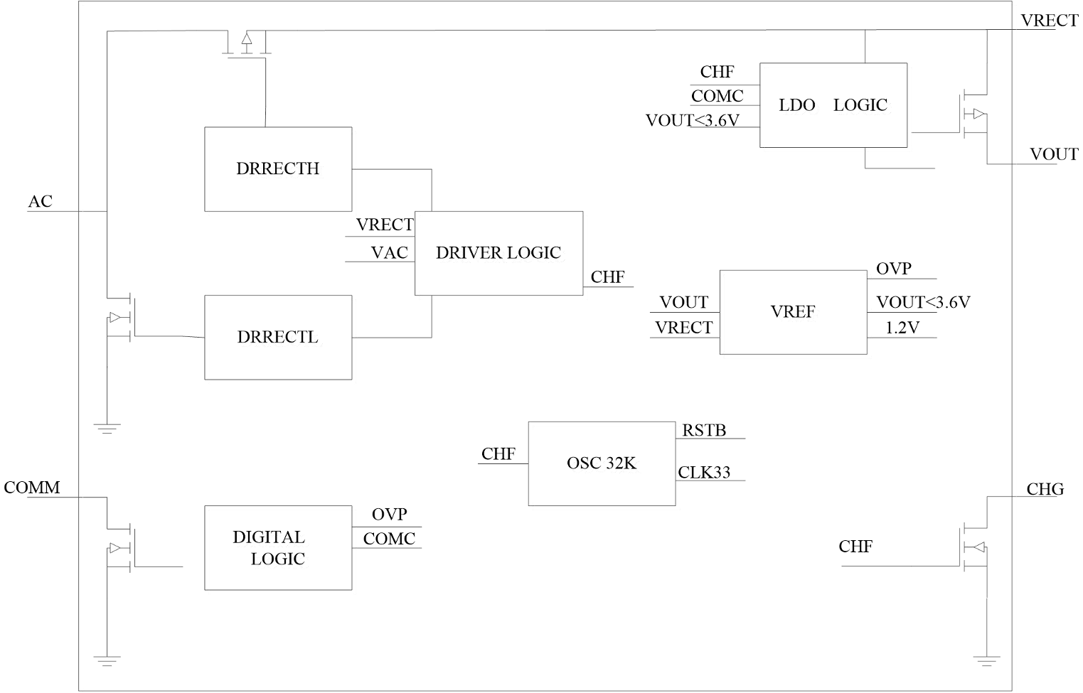 Figure 1: Internal block diagram showing the integration of the half-bridge and OVP logic.
Experiments & Performance Metrics
The chip's performance is optimized for the "Sleep-Charge-Run" cycle typical of small IoT devices.
- Ultra-Low Leakage: In standby (no AC signal), the current consumption is , crucial for maintaining battery health in long-shelf-life products.
- Thermal Robustness: The built-in Over-Temperature Protection (OTP) initiates at 150°C and recovers at 120°C, providing a significant 30°C hysteresis to prevent "thermal oscillation" during high-current charging.
- Voltage Versatility:
- JDS9007A: Fixed 5V output for standard USB-level logic.
- JDS9007B: Fixed 4.2V output, ideal for direct Li-ion battery charging paths.
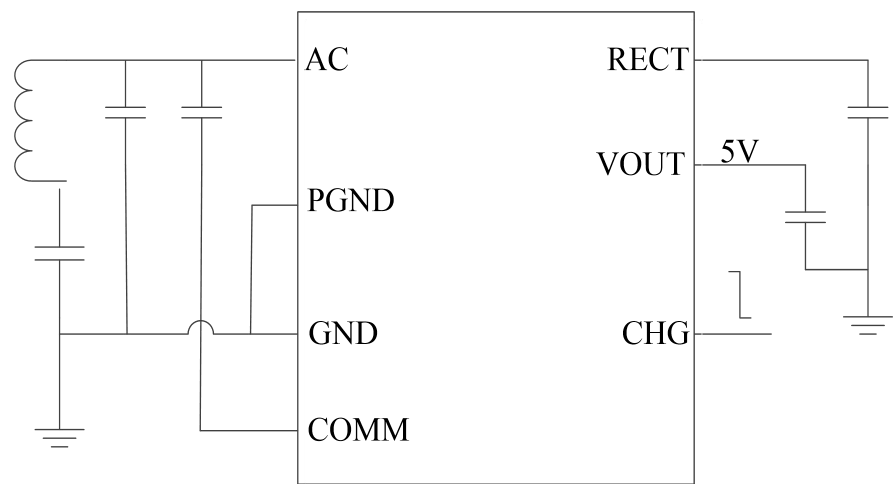 Figure 2: Minimal peripheral circuitry required for a complete wireless charging receiver.
Critical Analysis & Conclusion
Takeaway
The JDS9007X is a surgical solution for a specific problem: micro-scale wireless power. It avoids the "feature creep" of larger Qi-compliant chips to focus on size and simplicity.
Limitations
The maximum current is capped at 200mA, meaning it is not suitable for smartphones or tablets. Additionally, it uses a linear regulator (LDO) rather than a Buck converter; while this saves space and reduces EMI, the efficiency will drop if the input-to-output voltage gap (VRECT - VOUT) becomes too large.
Future Outlook
As the industry moves toward smart rings and bio-implants, we expect to see the JDS9007X's architecture evolve into even smaller packages (like WLCSP) and integrate more complex data-backscatter protocols without increasing the footprint.